
14. SEMI CONDUCTOR ELECTRONICS : MATERIALS, DEVICES & SIMPLE CIRCUITS (Long Answer Type Question)
Q. 1. What is energy ? Distinguis between conductor, semiconductor and insulator on the basis of energy band. How does the resistance of semiconductor varries with the change of the temperature, Explain.
Ans ⇒ Depending upon the relative positions of the valence band and the conduction band, the solids can be classfied into conductors, insultators and semic conductors.
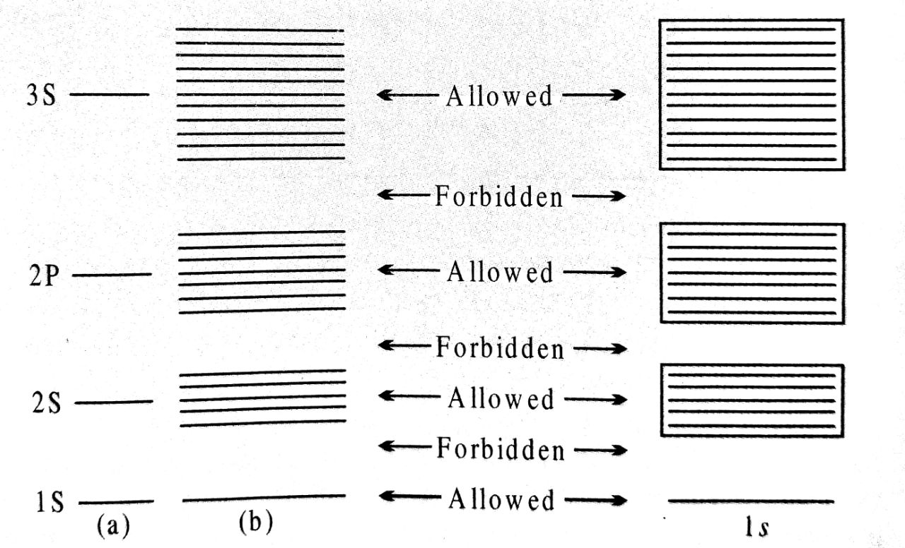
Band theory of Solids : By the help of band theory so solids metals, insulators and semiconductor can be classfied. the energy band diagram for metals is such that either the conduction band is partially filled with electrons or the conjuction and valence band partly overlap each other and there is no forbidden energy gap in between. From the band theory of solids the electons are tightly band with their nucleus. The energy level diagram of such type of atoms are shown in fig. (a). If such types of atoms combines them in each condition the corresponding energy level will be some different continious energy level of energy, as shown in fig. (b).
There are majority of electrons in the solids. Due to shich new energy levels are very closest throught wihch bonds are developed, as shown in fig. (c). The energy levels are continious in ls, 2s, 2p, 3s.
It the no. of atoms are N then for every 1 the corresponding ml-no. of conditions is (2l + 1) and for a given s are represented by two values for ms = (= ±1/2).
The formation of bands in different solids are different. Electrons can blive only in these states or can travell. These bands are shaded and called allowed bands. The mid area of the allowed bands are called forbidden rigions because electrons are not found in this band. Commonly the lower most band Alled up with electrons. The uppermost band which is partially or fully filled up with elecrons are called as valence band.
Conductors : The energy band diagram fo metals is such that either the conduction band is partially filled with electrons or the conduction and valence band partly overlap each other and there is no forbidden gap in between, as shown in fig, (c) and in fig. (d). In both the situations, it can be considered that the metal has a single energy band which is partly filled and partly empty. Even if a small electric field is applied across the metal. These free electrons start moving in a direction opposite to the direction of electric field. Due to it, a current begins to flow throught it and hence metal behaves as a conductor.
Semiconductors : The energy band diagram of semiconductors is shown in fig. (b), Here also, the valence band is totally fielled and the conduction band is emepty but the forbidden gap between conduction band and valence band is quite small. It is about iev. for example, the forbidden gap for germanium is of 0.72 eV and for silicon it is of 1.1ev. at zero kelvine electrons are not able to cross even this small forbidden gap and hence othe conduction band remains totally empty. Therefore the semiconductors at zero kelvin behaves as insulator.
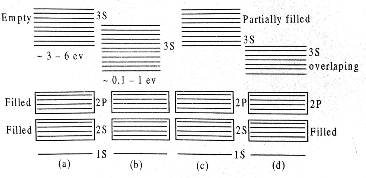
However at room temperature, some electrons in the valence band acquire thermal energy greater than energy gap of lev and jump over to the conduction band where they are free to move under influlence of even a small electric field. As a results of it, the semiconductor acquires small conductivity at room temperature.
Insulators : The energy band dlagrain is shown in the above fig. (a) Here, the valence band is completely filled, Here, the valence band is completely filled, the conduction band is empty and forbidderi gap is quite large. For example in case of diarnond. the forbidden gap is Gev. Since the valence hand is completely filled as per Pauli’s exclusion principle, therefor the electrons are not free. Again due to large forbidden gap, no electrons is able to go from the valence band to the conduction band even if electric field is pplied. Hence electrical conduction in these materials is impossible and they behave as insulators.
Effect of temperature on semiconductors : The resistance of any semi conductor varies with the change of temperatures. As the temperature increases the resistance of semiconductor decreases and vice versa.
Q.2. Draw the Input/Output characteristic curve in CE mode. What do we understand by the cut off, active and saturation states of the transistor ?
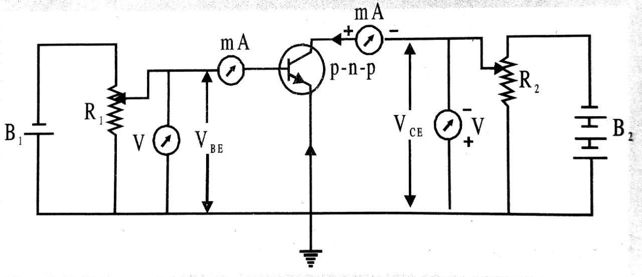
Ans ⇒ Circuit diagram to study the common emitter characteristics of a transistor is shown in figure A.
Input characteristics :
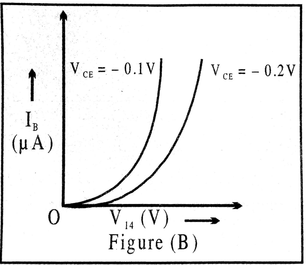
The variation of base current Ib (input) with base emitter voltage (VEB) at constant collector-emitter coltage (VCE) is called input characteristics.
The input characteristics are similar to forward bias characteristics of a junction diode.
For a given value of emitter-base voltage (VBE), the base current d-emitter voltage.
Output characteristics :
The variation of the collector current Ic (output) with collector-emitter voltage (VCE) at constant base current (Ib) is called output characteristic.
For a given value of base current, collector current increases rapidly with the collector-emitter voltage in the beginning but at high value of VCE’ collector current becomes constant.
For a given value of VCE’ the collector current (IC) is higher for high value of base current (Ib).
When used as a switch the transistor does not remain in active region. Active region is used during Transistor Amplifier. Output characteristics of a transistor in common-emitter configuration are divided into following three regions :
(i) Active region : Active region lies above IB = O as shown in figure. In this region, collector junction is reverse biased and emitter junction is forward biased. For a given value of IB. collector current increases as (VCE) increases.
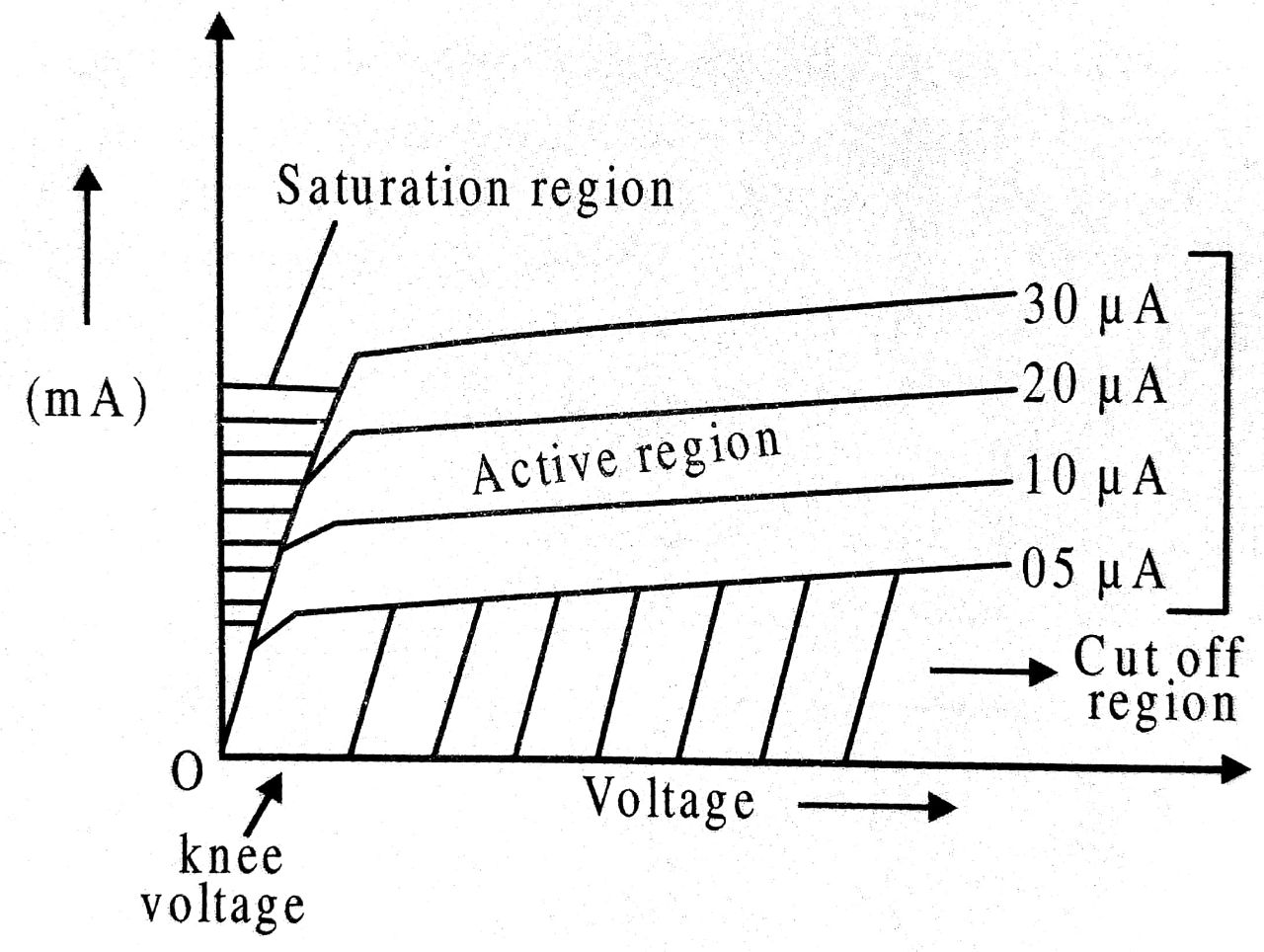
(ii) Cut off region : The collector current has finite value under this condition. In order of cut off the transistor, the emitter junction has to be made slightly reverse biased in addition to IB = 0.
(iii) Saturation region : Saturation region lies close to zero voltage axis where all the curves coincide. In this region, collector current is independent of the base current.
When used as a switch the transistor does not remain in active region. Active region is used during Transistor Amplifier.
Q.3. Explain (i) Forward biasing (ii) reverse biasing of a p-n junction diode. With the help of a circuit diagram, explain the use of this device as a rectifier.
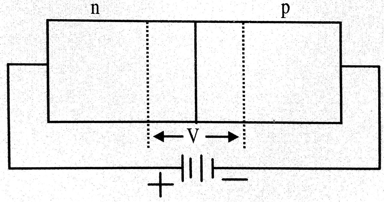
Ans ⇒ (i) Forward biasing of PN junction diode :
A pn junction is said to be forward if an external battery of emf greater than the potential barrier (Vb) is connected to pn junction in such a way that tive terminal of the external battery is connected to p side and -ve terminal to n-side of the junction diode.
In forward biasing, applied forward potential establishes an electric field which acts opposite to field due to potential barrier. Therefore resultant field is weak end due to which potential barrier is considerably reduced and hence the depletion layer becomes thin. As a result a low resistance path is established for entire circuit. Thus current flows in the circuit. This current is called forward current.
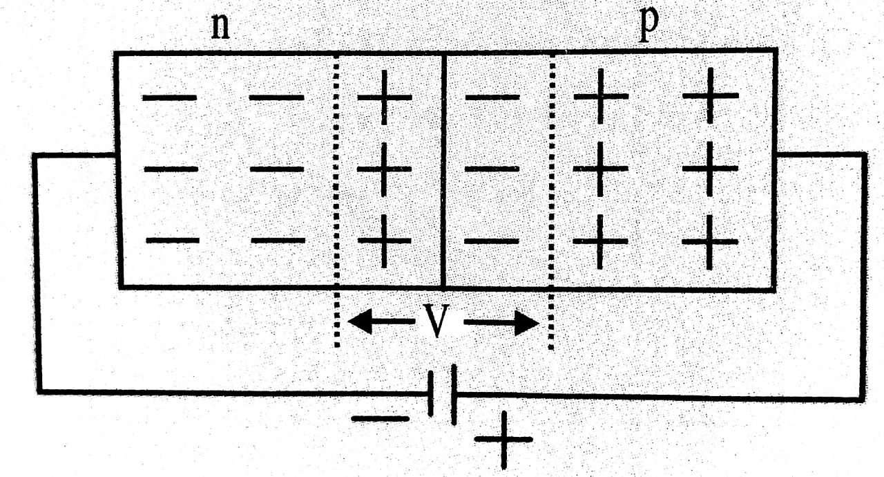
(ii) Reverse biasing of pn junction diode :
A pn junction is said to be reverse biased if the +ve terminal of external battery is connected to n side of the junction on diode and -ve terminal is connected to p-side of diode.
In reverse biasing, applied reverse voltage establishes an electric field in same direction of potential barrier. The reverse voltage supports it, as a result majority charge carriers are pulled a way from the junction and hence depletion layer increases. Therefore a high resistance path is established for the entire circuit and hence no current flows in the circuit. i.e. in reverse biasing of diode no current does not flows in the circuit.
PN Junction diode as half wave rectifier :
The rectifier, which converts only one half of a.c. intput into d.c. is called half wave rectifier.
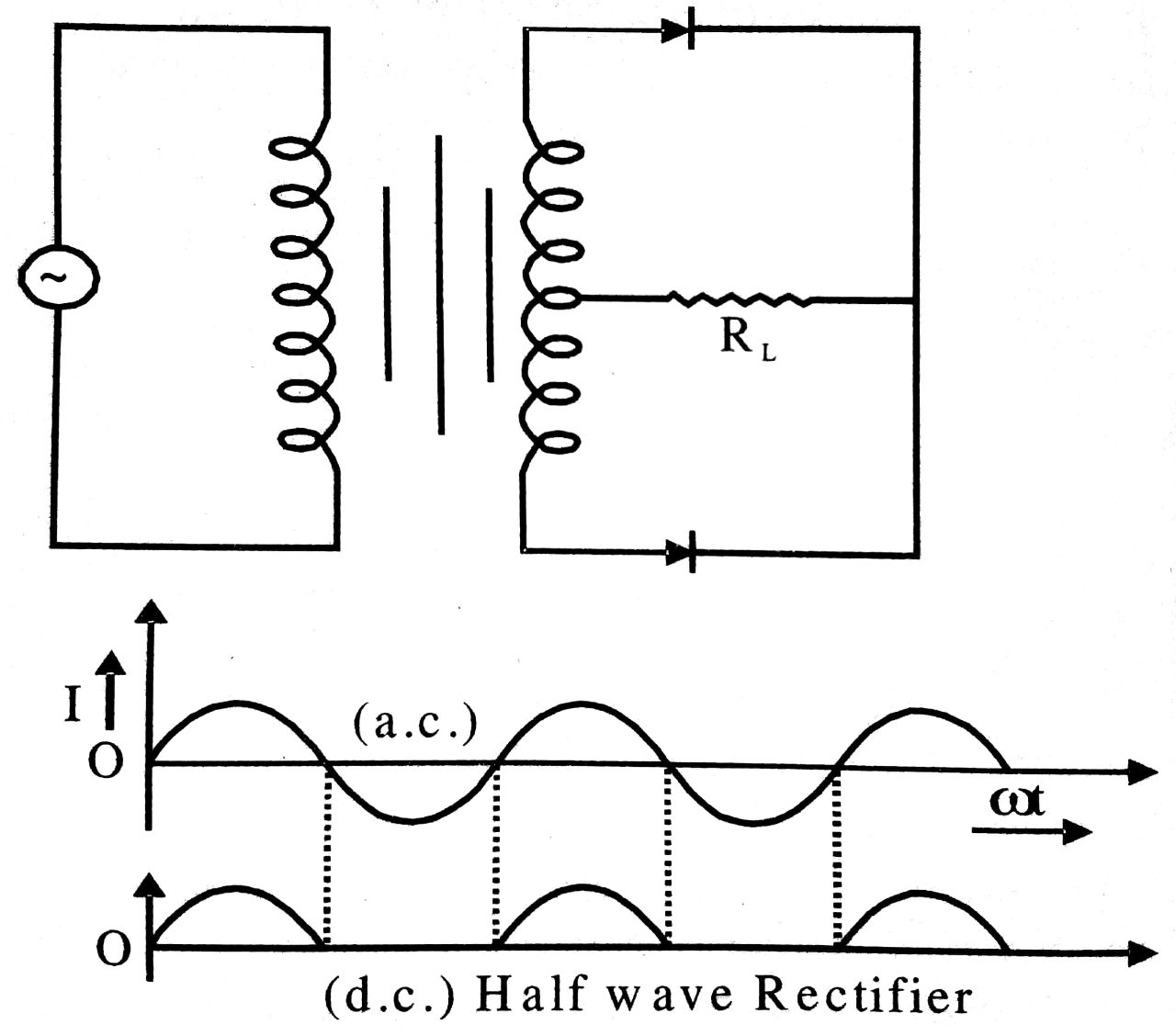
During +ve half cycle of the a.c. input voltage the diode is forward biased and current flows through load RL. This current developes a voltage across load PL.
During-ve half cycle pf the a.c. input, diode is reverse biased. No current flows in the circuit and hence no voltage is developed across load RL.
Thus alternating voltage fed to primary coil (P) of transformer (Tr) appears as pulsating d.c. across the output load RL. Since voltage across the load appears only during +ve half cycle of the input a.c. the other half is missing, thus this process is called half wave rectification and the arrangement used is called half wave rectifier.
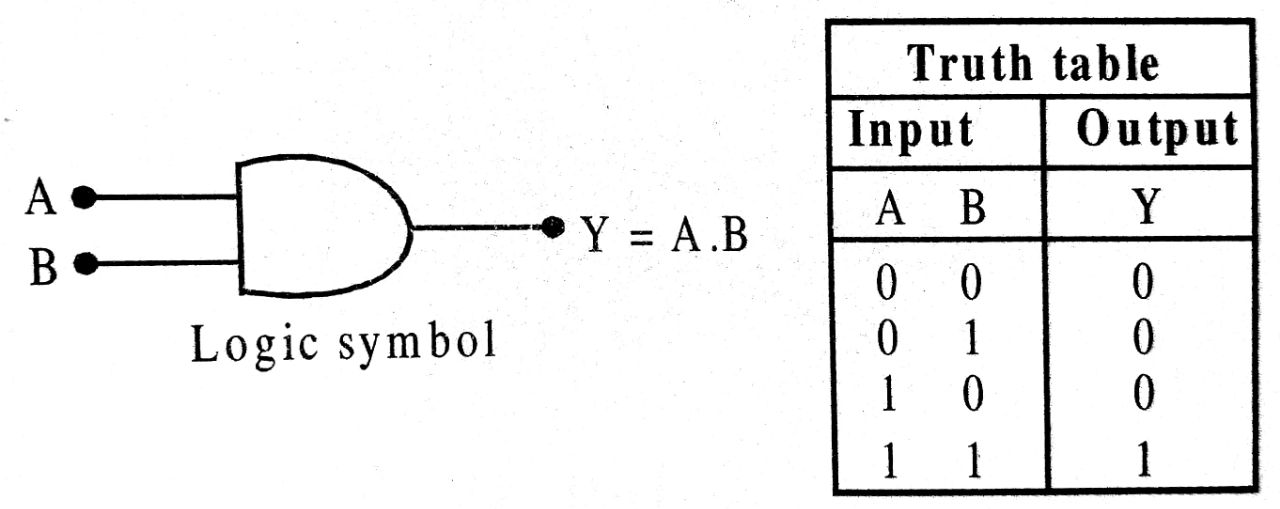
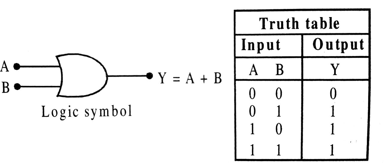
Q.4. What are logic gates (OR, AND & NOT)? Discuss them with truth table.
Ans ⇒ Logic gates : These are such circuit which establish a relation between input & output. Mainly there are three OR gates, AND gate and NOT gates. Others are obtained by their combination (NOR, NAND, XOR etc).
AND gate : It is two input & one output gate. It represents the multiplication operation. The Boolean expression for this gate is Y = 4.B which is read as Y equals A and B.
OR gate : It is also two input & are output gate. The Boolean expression for this operation is Y = A + B. It is read as Y equal A OR B.
NOT gate : It is one input & one output gate. It inverses the input. Its Boolean expression = Y = Ā.
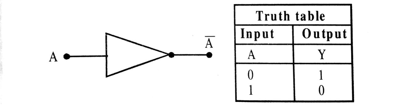
In output there is a small circle which is called invert bubble.
Class 12th physics Long Type question in English
| S.N | Physics Long Type Question English Medium |
| 1. | ELECTRIC CHARGES AND FIELDS |
| 2. | LECTROSTATIC POTENTIAL AND CAPACITANCE |
| 3. | CURRENT ELECTRICITY |
| 4. | MOVING CHARGES AND MAGNETISM |
| 5. | MAGNETISM AND MATTER |
| 6. | ELECTROMAGNETIC INDUCTION |
| 7. | ALTERNATING CURRENT |
| 8. | ELECTROMAGNETIC WAVES |
| 9. | RAY OPTICS AND OPTICAL INSTRUMENTS |
| 10. | WAVE OPTICS |
| 11. | DUAL NATURE OF MATTER AND RADIATION |
| 12. | ATOMS |
| 13. | NUCLEI |
| 14. | SEMI CONDUCTOR ELECTRONICS |
| 15. | COMMUNICATION SYSTEMS |