
14. SEMI CONDUCTOR ELECTRONICS : MATERIALS, DEVICES & SIMPLE CIRCUITS TILE ( SHORT QUESTION ANSWER 2022 )
14. SEMI CONDUCTOR ELECTRONICS : MATERIALS, DEVICES & SIMPLE CIRCUITS TILE
Q.1. Distinguish between an intrinsic semiconductor and p-type semiconductor. Give reason, why, any type of semiconductor crystal is electrically neutral, although nh >> ne ?
Ans ⇒ (i) Intrinsic semiconductor is a pure semiconductor free from any impurity. P-type semiconductor contains a trivalent impurity (it is a doped semiconductor).
(ii) P-type semiconductor is in fact neutral intrinsic semiconductor neutral trivalent impurity is added to neutral pure semiconductor crystal.
Q.2. Explain the formation of potential barrier and depletion region, in p-n junction.
Ans ⇒ When P type and N type semiconductors are joined together, the majority charge carriers i.e. holes in P type semiconductor and free electrons in N type semiconductor cross over the PN junction. The region donating the electron becomes +ve charge and the region accepting the electron becomes
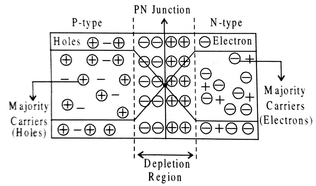
-ve charge. The process of migration of charge carriers go on till a region as shown in the adjoining figure is formed which further stops the cross over of electrons and holes. This region is known as depletion layer or depletion region. Thickness of this layer is about 10-3 m. The recombination of holes and electrons near the junction results into accumulation of +ve and -ve charges near the junction. Thus a potential difference occurs near about the junction. The value of this potential difference is about 0.5V. Since this potential does not allow further recombination of holes and free electrons, therefore, it is known as potential barrier.
Q.3. What is an intrinsic semiconductor ? How can the material be converted into (i) p-type (ii) n-type extrinsic semiconductor ? Explain with the help of energy band diagrams.
Ans ⇒ Intrinsic semiconductor is a pure semiconductor which is free from any impure atoms.
Intrinsic semiconductor can be converted into n-type semiconductor by doping it with atoms belonging to V group of the periodic table such as phosphorus or arsenic.
conversion in p-type semiconductor : Intrinsic semi conductor can be converted into p-type semiconductor by doping of the impure atoms of III group of periodic table such as In, B or Al or gallium.
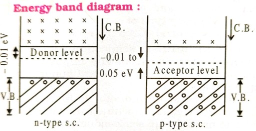
Hence in n-type majority charge carrier are electrons due to doping of pentavalent impurity and in p-type semiconductor majority charge carries are holes.
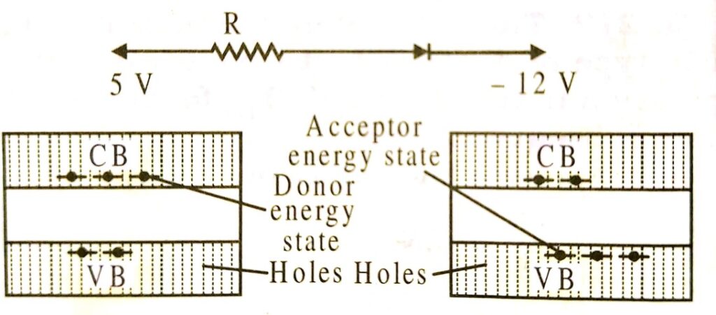
Q.4. Draw the energy band diagram of (i) n-type and (ii) p-type semiconductor. State whether the ideal diode shown is forward biased or reverse biased and find the voltage it.
Ans ⇒
 Energy band structure of n-type
and p-type semiconductor Forward biased.
Anode — 5 V and cathode — 12 V (Low)
i.e., P-side is at higher potential.
Q.5. What do you mean by doping ?
Ans ⇒ It is the process of mixing impurity in a semiconductor. Germanium is tetravalent if a pentavalent material is mixed in it then newly formed material is n-type. Ge+ Arsenic (impurity).
Similarly, by mixing indium with germanium p type semiconductor is formed.
Q.6. Give differences among valence band, conduction band and forbidden band.
Ans ⇒ In valence energy band there are electrons. It is partially or fully filled with electrons. It is never vacant. In this band electrons have no capacity to take electrons from outer electric field. Electrons present in this band does not contribute to flow of electrons.
In conduction band electrons are rarely present. It is partially filled with electrons or completely empty. Electrons in this band receives energy from electric field. They contribute in flow of electric current.
In forbidden energy gap electrons are not present. It is fully empty. To shift electrons from valence band to conduction band energy is needed which is called band gap energy (Eg).
Q.7. What is LED ? What are its applications ?
Ans ⇒ It is short form of light emitting diode. Its action is based on conversion of electric into light energy. It is generally p-n junction diode in which gallium arsenide or indium phosphide is used as semiconductor.
Due to combination of holes and electrons at junction, energy is librated. In this process light emitted by it is of visible range (wavelength). It is generally used in burglar alarm, calculators, pilot lamps, telephone, digital watches and in switch board.
Q.8. n-p-n transistors are used more than that of p-n-p transitors. Why ?
Ans ⇒ In n-p-n transistors maior current carriers are free electrons. But in p-n-p major carries are holes. Ionic mobility of electrons is more than holes. So, n-p-n transistors are preferred more than p-n-p.
Class 12th physics Subjective question in English
| S.N | Physics Short Type Question English Medium |
| 1. | ELECTRIC CHARGES AND FIELDS |
| 2. | LECTROSTATIC POTENTIAL AND CAPACITANCE |
| 3. | CURRENT ELECTRICITY |
| 4. | MOVING CHARGES AND MAGNETISM |
| 5. | MAGNETISM AND MATTER |
| 6. | ELECTROMAGNETIC INDUCTION |
| 7. | ALTERNATING CURRENT |
| 8. | ELECTROMAGNETIC WAVES |
| 9. | RAY OPTICS AND OPTICAL INSTRUMENTS |
| 10. | WAVE OPTICS |
| 11. | DUAL NATURE OF MATTER AND RADIATION |
| 12. | ATOMS |
| 13. | NUCLEI |
| 14. | SEMI CONDUCTOR ELECTRONICS |
| 15. | COMMUNICATION SYSTEMS |