14. SEMI CONDUCTOR ELECTRONICS : ATERIALS, DEVICES & SIMPLE CIRCUITS( Objective Question Answer 2022 )
1. Bonds in a semiconductor :
(A) trivalent
(B) covalent
(C) bivalent
(D) monovalent
| Answer ⇒ B |
2. Number of electrons in the valence shell of a semiconductor is :
(A) 1
(B) 2
(C) 3
(D) 4
| Answer ⇒ D |
3. Semiconductors of both p-type and n-type are produced by :
(A) ionic solids
(B) covalent solids
(C) metallic solids
(D) molecular solids
| Answer ⇒ B |
4. With fall of temperature, the forbidden energy gap of a semiconductor
(A) increases
(B) decreases
(C) remains unchanged
(D) sometimes increases and sometimes decreases
| Answer ⇒ C |
5. In a p-type semiconductor, current conduction is by :
(A) atoms
(B) holes
(C) electrons
(D) protons
| Answer ⇒ B |
6. The relation between number of free electrons (n) in a semiconductor and temperature (T) is given by :
(A) n ∝ T
(B) n ∝ T2
(C) n ∝ T1/2
(D) n ∝ T3/2
| Answer ⇒ D |
7. In reverse biasing :
(A) large amount of current flows
(B) no current flows
(C) potential barrier across junction increases
(D) depletion layer resistance increases
| Answer ⇒ C |
8. Main function of a transistor is to :
(A) rectify
(B) simplify
(C) amplify
(D) all the above
| Answer ⇒ C |
9. In semi conductor, at room temperature :
(A) the valence bond is partially empty and the conduction band is partially filled
(B) the valence band is completely filled and the conduction band is partially filled
(C) the valence band is completely filled
(D) the conduction band is completely empty
| Answer ⇒ A |
10. Crystal diode is :
(A) amplifying device
(B) fluctuating device
(C) non-linear device
(D) linear device
| Answer ⇒ C |
11. The part of a transistor which is heavily doped to produce a large number of majority carriers is :
(A) base
(B) emitter
(C) collector
(D) None of these
| Answer ⇒ B |
12. A p-type semiconductor is :
(A) negatively charged
(B) positively charged
(C) uncharged
(D) None of these
| Answer ⇒ C |
13. In ne, nh, nt, Nd and Na respectively denote number density of electrons, number density of holes, number density of intrinsic carriers, density of donor atoms, density of acceptor atoms in a semiconductor, we can write :
(A) nenh = ni2
(B) nenh = ni
(C) neni = nh
(D) neni = (ne + ni)nh
| Answer ⇒ A |
14. Refer to previous question :
(A) ne = Nd >> nh
(B) nh = Na = ne
(C) nh = Nd + Na = ne
(D) nenh = NdNa
| Answer ⇒ A |
15. The ‘device used to convert“ alternating voltage/current into direct voltage/current is called :
(A) rectifier
(B) amplifier
(C) oscillator
(D) None of these
| Answer ⇒ A |
16. If nh and ne are the number of holes and electrons, is an intrinsic semiconductor :
(A) nh > ne
(B) nh = ne
(C) nh > ne
(D) hh ≠ En
| Answer ⇒ B |
17. Band gap in germanium and silicon is eV are :
(A) 0.78, 1.17
(B) 1.1, 0.7
(C) 11,0
(D) 0,1,1
| Answer ⇒ A |
18. In a common base configuration of a transistor ![]() then; current gain in common emitter configuration of transistor will be :
then; current gain in common emitter configuration of transistor will be :
(A) 49
(B) 98
(C) 4.9
(D) 24.5
| Answer ⇒ A |
19. The correct relation between the two current gains ∝ and β in a transistor is :
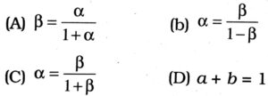
| Answer ⇒ C |
Class 12th physics objective question in English
| S.N | Physics Objective English Medium |
| 1. | ELECTRIC CHARGES AND FIELDS |
| 2. | LECTROSTATIC POTENTIAL AND CAPACITANCE |
| 3. | CURRENT ELECTRICITY |
| 4. | MOVING CHARGES AND MAGNETISM |
| 5. | MAGNETISM AND MATTER |
| 6. | ELECTROMAGNETIC INDUCTION |
| 7. | ALTERNATING CURRENT |
| 8. | ELECTROMAGNETIC WAVES |
| 9. | RAY OPTICS AND OPTICAL INSTRUMENTS |
| 10. | WAVE OPTICS |
| 11. | DUAL NATURE OF MATTER AND RADIATION |
| 12. | ATOMS |
| 13. | NUCLEI |
| 14. | SEMI CONDUCTOR ELECTRONICS |
| 15. | COMMUNICATION SYSTEMS |